|
| |
nextnano3 - Tutorial
next generation 3D nano device simulator
1D Tutorial
k|| energy dispersion of holes in unstrained and strained silicon inversion
layers
Authors:
Stefan Birner, Michael
Povolotskyi (University of Rome "Tor Vergata")
If you want to obtain the input files that are used within this tutorial, please
check if you can find them in the installation directory.
If you cannot find them, please submit a
Support Ticket.
-> 1DSi_triangular_unstrained_001surface.in -
for [001] surface, unstrained, compressive strain, tensile strain
-> 1DSi_triangular_unstrained_011surface.in -
-> 1DSi_triangular_unstrained_111surface.in -
-> 1DSi_triangular_strained_uniaxial_comp_001surface_read_in_strain.in
-
for [001] surface, compressive strain uniaxial along [110]
Uniaxial strain file to be read in:
strain_cr1D_read_in_uniaxial110_1GPa.dat
k|| energy dispersion of holes in of unstrained and strained p-channel silicon inversion
layers
This tutorial aims to reproduce the figures presented in
M. Fischetti, Z. Ren, P.M. Solomon, M. Yang, K. Rim
Six-band k.p calculation of the hole mobility in
silicon inversion layers: Dependence on surface orientation, strain, and silicon
thickness
J. Appl. Phys. 94 (2), 1079 (2003)
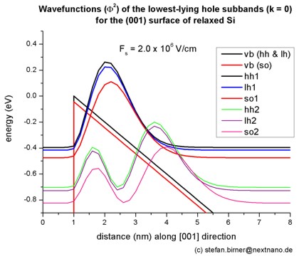
Step 1: Unstrained silicon inversion layer with (001) surface orientation
-> 1DSi_triangular_unstrained_001surface.in
- The following figure shows the valence band edges (where the heavy and
light hole band edges are degenerate) and the six lowest hole wave functions of a Si
inversion layer (triangular-well approximation) for k = 0 (i.e. kx
= ky = 0) where the z axis is oriented along the [001]
direction.
The potential energy of the well is given by V(z') = e Fs z'
where Fs is the surface field. In the figure, the electric field is
Fs = -2000 kV/cm.
Note that in the figure z is shifted by 1 nm: V(z=1) = V(z'=0).
One can clearly distinguish the holes by their character (heavy-hole-like,
light-hole-like, split-off-hole-like).
- The following figure aims to reproduce Fig. 1(a) of Fischetti's paper.
The energies of the six lowest-lying hole subbands for the (001) surface of
unstrained Si inversion layer are plotted as a function of applied electric
field (i.e. as a function of the triangular-well potential).
The subband energies are measured from the surface potential.
Our results are in excellent agreement with Fischetti's results.
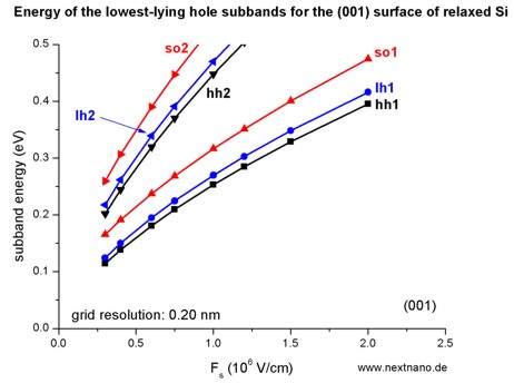
The symbols are calculated values, the connecting lines only a guide to the
eye.
The hole energies are taken to be positive, in contrast to the figure above
showing the wave functions and the valence band edges.
The labels of the curves (hh, lh
and so) are taken from Fischetti's paper.
We do not perform this analysis within nextnano³ because it is not
important for quantitative results.
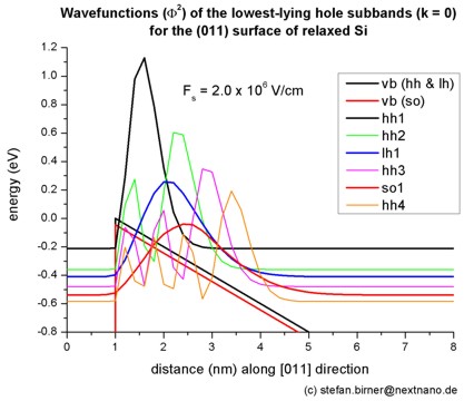
Step 2: Unstrained silicon inversion layer with (011) surface orientation
-> 1DSi_triangular_unstrained_011surface.in
- The following figure shows the valence band edges (where the heavy and
light hole band edges are degenerate) and the six lowest hole wave functions of a Si
inversion layer (triangular-well approximation) for k = 0 (i.e. kx
= ky = 0) where the z axis is oriented along the [011]
direction.
The potential energy of the well is given by V(z') = e Fs z'
where Fs is the surface field. In the figure, the electric field is
Fs = -2000 kV/cm.
Note that in the figure z is shifted by 1 nm: V(z=1) = V(z'=0).
One can clearly distinguish the holes by their character (heavy-hole-like,
light-hole-like, split-off-hole-like).
- The following figure aims to reproduce Fig. 2(a) of Fischetti's paper.
The energies of the six lowest-lying hole subbands for the (011) surface of
unstrained Si inversion layer are plotted as a function of applied electric
field (i.e. as a function of the triangular-well potential).
The subband energies are measured from the surface potential.
Our results are in excellent agreement with Fischetti's results.
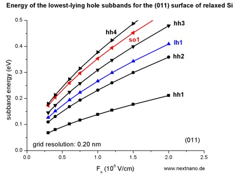
The symbols are calculated values, the connecting lines only a guide to the
eye.
The hole energies are taken to be positive, in contrast to the figure above
showing the wave functions and the valence band edges.
The labels of the curves (hh, lh
and so) are taken from Fischetti's paper.
We do not perform this analysis within nextnano³ because it is not
important for quantitative results.
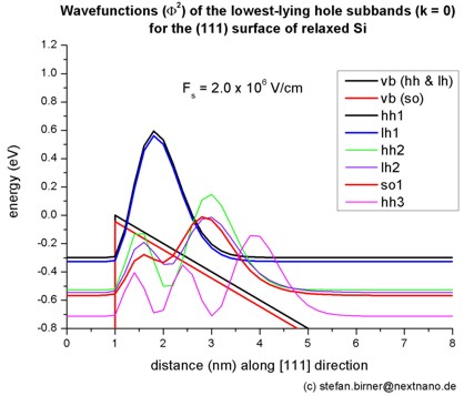
Step 3: Unstrained silicon inversion layer with (111) surface orientation
-> 1DSi_triangular_unstrained_111surface.in
- The following figure shows the valence band edges (where the heavy and
light hole band edges are degenerate) and the six lowest hole wave functions of a Si
inversion layer (triangular-well approximation) for k = 0 (i.e. kx
= ky = 0) where the z axis is oriented along the [111]
direction.
The potential energy of the well is given by V(z') = e Fs z'
where Fs is the surface field. In the figure, the electric field is
Fs = -2000 kV/cm.
Note that in the figure z is shifted by 1 nm: V(z=1) = V(z'=0).
- The following figure aims to reproduce Fig. 3(a) of Fischetti's paper.
The energies of the six lowest-lying hole subbands for the (111) surface of
unstrained Si inversion layer are plotted as a function of applied electric
field (i.e. as a function of the triangular-well potential).
The subband energies are measured from the surface potential.
Our results are in excellent agreement with Fischetti's results.
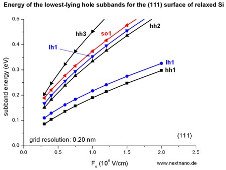
The symbols are calculated values, the connecting lines only a guide to the
eye.
The hole energies are taken to be positive, in contrast to the figure above
showing the wave functions and the valence band edges.
The labels of the curves (hh, lh
and so) are taken from Fischetti's paper.
We do not perform this analysis within nextnano³ because it is not
important for quantitative results.
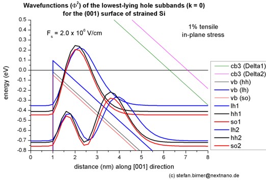
Step 4: Tensilely strained silicon inversion layer with (001) surface orientation
-> 1DSi_triangular_unstrained_001surface.in - (Hint:
Modify %SubstrateLatticeConstant in input file.)
- The following figure shows the valence band edges (where the heavy and
light hole band edges are no longer degenerate) and the six lowest hole wave functions of a
tensilely strained Si
inversion layer (triangular-well approximation) for k = 0 (i.e. kx
= ky = 0) where the z axis is oriented along the [001]
direction. The tensile in-plane strain in the (x,y) plane is 1%. This
correspond to a Si0.75Ge0.25 substrate.
The potential energy of the well is given by V(z') = e Fs z'
where Fs is the surface field. In the figure, the electric field is
Fs = -2000 kV/cm.
Note that in the figure z is shifted by 1 nm: V(z=1) = V(z'=0).
- The following figure aims to reproduce Fig. 5(a) of Fischetti's paper.
The energies of the six lowest-lying hole subbands for the (001) surface of
the tensilely strained Si inversion layer are plotted as a function of applied electric
field (i.e. as a function of the triangular-well potential).
The subband energies are measured from the surface potential which is assumed
to be at 0 eV for the unstrained valence band edges.
After application of strain, the highest valence band edge is the
light hole band edge at 96.72 meV
(compare with straight line in the figure above).
Our results are in excellent agreement with Fischetti's results.
At low fields (-300 kV/cm and -400 kV/cm), the third hole eigenstate is the
second light hole state (lh2) whereas for
higher fields this is the split-off hole state (so1).
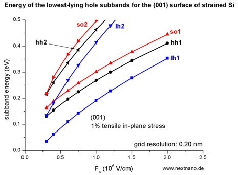
The symbols are calculated values, the connecting lines only a guide to the
eye.
The hole energies are taken to be positive, in contrast to the figure above
showing the wave functions and the band edges.
The labels of the curves (hh, lh
and so) are taken from Fischetti's paper.
We do not perform this analysis within nextnano³ because it is not
important for quantitative results.
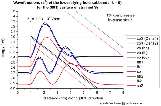
Step 5: Compressively strained silicon inversion layer with (001) surface orientation
-> 1DSi_triangular_unstrained_001surface.in - (Hint:
Modify %SubstrateLatticeConstant in input file.)
- The following figure shows the valence band edges (where the heavy and
light hole band edges are no longer degenerate) and the six lowest hole wave functions of a
compressively strained Si
inversion layer (triangular-well approximation) for k = 0 (i.e. kx
= ky = 0) where the z axis is oriented along the [001]
direction. The compressive in-plane strain in the (x,y) plane is 1%.
The potential energy of the well is given by V(z') = e Fs z'
where Fs is the surface field. In the figure, the electric field is
Fs = -2000 kV/cm.
Note that in the figure z is shifted by 1 nm: V(z=1) = V(z'=0).
- The following figure aims to reproduce Fig. 6(a) of Fischetti's paper.
The energies of the six lowest-lying hole subbands for the (001) surface of
the compressively strained Si inversion layer are plotted as a function of applied electric
field (i.e. as a function of the triangular-well potential).
The subband energies are measured from the surface potential which is assumed
to be at 0 eV for the unstrained valence band edges.
After application of strain, the highest valence band edge is the heavy
hole band edge at 15.47 meV (compare with straight line in the figure
above).
Our results are in excellent agreement with Fischetti's results.
Again, we have crossings of the subbands. At small confining fields, the
effect of confinement is compensated by the effect of strain.
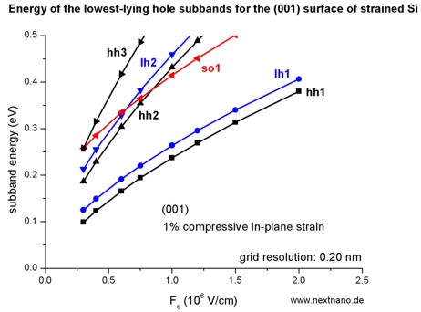
The symbols are calculated values, the connecting lines only a guide to the
eye.
The hole energies are taken to be positive, in contrast to the figure above
showing the wave functions and the band edges.
The labels of the curves (hh, lh
and so) are taken from Fischetti's paper.
We do not perform this analysis within nextnano³ because it is not
important for quantitative results.
Step 6: k|| dispersion of unstrained silicon inversion layer with (001)
surface orientation
-> 1DSi_triangular_unstrained_001surface.in
- The following figure aims to reproduce Fig. 4(a) of Fischetti's paper.
It shows the equienergy lines of the lowest lying
heavy hole, light hole and split-off hole subbands
for the (001) surface of unstrained silicon. Only one spin
state is plotted for clarity.
The x and y axes represent kx and ky in units of
[1/Angstrom]. The x axis points along the [100], the y axis along the [010]
direction of the crystal coordinate system.
The equienergy lines are plotted for E - E0 = 25 meV
where E0 is the eigenvalue of the corresponding subbands at k
= (kx,ky) = 0.
The electric field was taken to be Fs = -1000 kV/cm.
The eigenvalues are spin-degenerate only at k = (kx,ky)
= 0 but differ for non-zero k. The plots show the k||
dispersions of the lowest heavy hole (1st eigenstate), the lowest
light hole (3rd eigenstate) and the lowest split-off hole (5th
eigenstate).
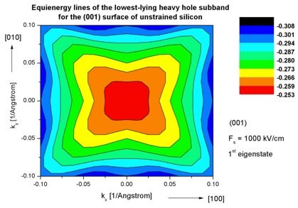 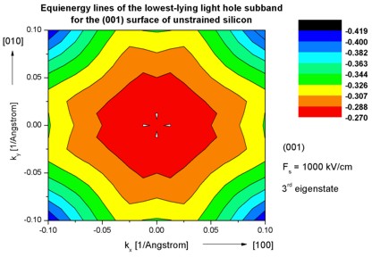
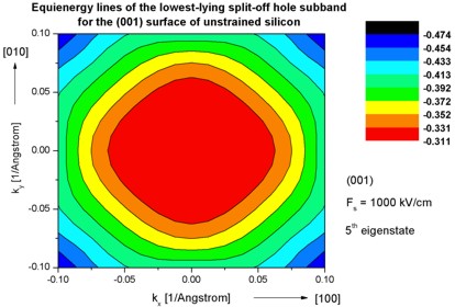
The left figure shows the dispersion for 1681 k|| points,
the right figure has a lower resolution of 361 k|| points.
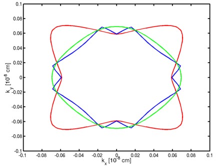
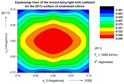
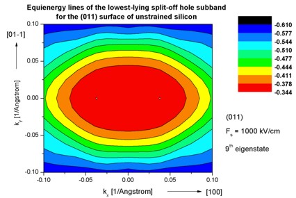
Step 7: k|| dispersion of unstrained silicon inversion layer with (011)
surface orientation
-> 1DSi_triangular_unstrained_011surface.in
- The following figures aim to reproduce Fig. 4(b) of Fischetti's paper.
It shows the equienergy lines of the lowest lying heavy hole, light hole and split-off hole subbands
for the (011) surface of unstrained silicon. Only one spin
state is plotted for clarity.
The x and y axes represent kx and ky in units of
[1/Angstrom]. The x axis points along the [100], the y axis along the [01-1]
direction of the crystal coordinate system.
The electric field was taken to be Fs = -1000 kV/cm.
The eigenvalues are spin-degenerate only at k = (kx,ky)
= 0 but differ for non-zero k. The plots show the k||
dispersions of the lowest heavy hole (1st eigenstate), the lowest
light hole (5th eigenstate) and the lowest split-off hole (9th
eigenstate).
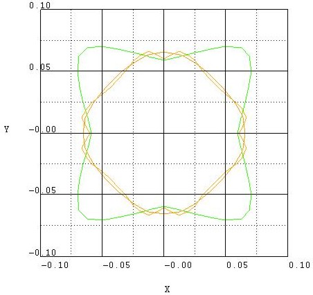
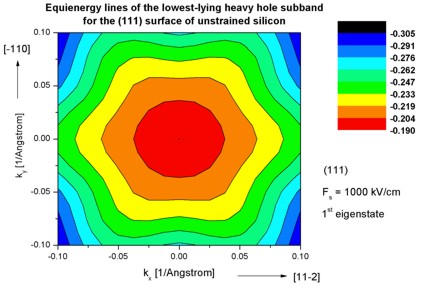
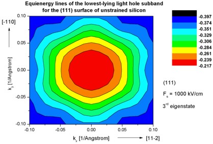
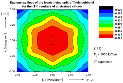
Step 8: k|| dispersion of unstrained silicon inversion layer with
(111)
surface orientation
-> 1DSi_triangular_unstrained_111surface.in
- The following figures aim to reproduce Fig. 4(c) of Fischetti's paper.
It shows the equienergy lines of the lowest lying heavy hole, light hole and split-off hole subbands
for the (111) surface of unstrained silicon. Only one spin
state is plotted for clarity.
The x and y axes represent kx and ky in units of
[1/Angstrom]. The x axis points along the [11-2], the y axis along the [-110]
direction of the crystal coordinate system.
The electric field was taken to be Fs = -1000 kV/cm.
The eigenvalues are spin-degenerate only at k = (kx,ky)
= 0 but differ for non-zero k. The plots show the k||
dispersions of the lowest heavy hole (1st eigenstate), the lowest
light hole (3rd eigenstate) and the lowest split-off hole (9th
eigenstate).
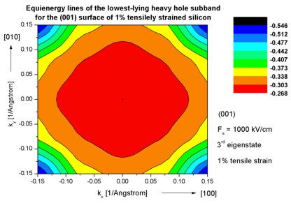
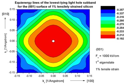
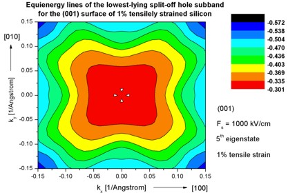
Step 9: k|| dispersion of 1% tensilely strained silicon inversion
layer with (001)
surface orientation
-> 1DSi_triangular_unstrained_001surface.in -
(Hint: Modify %SubstrateLatticeConstant in input file.)
- The following figures aim to reproduce Fig. 7(a) of Fischetti's paper.
It shows the equienergy lines of the lowest lying light hole, heavy hole and split-off hole subbands
for the (001) surface of 1% tensilely strained silicon. Only one spin
state is plotted for clarity.
The x and y axes represent kx and ky in units of
[1/Angstrom]. The x axis points along the [100], the y axis along the [010]
direction of the crystal coordinate system.
The electric field was taken to be Fs = -1000 kV/cm.
The eigenvalues are spin-degenerate only at k = (kx,ky)
= 0 but differ for non-zero k. The plots show the k||
dispersions of the lowest light hole (1st eigenstate), the lowest
heavy hole (3rd eigenstate) and the lowest split-off hole (5th
eigenstate).
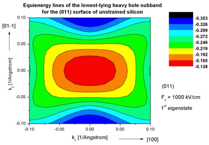
Step 10: k|| dispersion of 1% compressively strained silicon
inversion layer with (001)
surface orientation
-> 1DSi_triangular_unstrained_001surface.in -
(Hint: Modify %SubstrateLatticeConstant in input file.)
- The following figures aim to reproduce Fig. 7(b) of Fischetti's paper.
It shows the equienergy lines of the lowest lying heavy hole, light hole and split-off hole subbands
for the (001) surface of 1% compressively strained silicon. Only one spin
state is plotted for clarity.
The x and y axes represent kx and ky in units of
[1/Angstrom]. The x axis points along the [100], the y axis along the [010]
direction of the crystal coordinate system.
The electric field was taken to be Fs = -1000 kV/cm.
The eigenvalues are spin-degenerate only at k = (kx,ky)
= 0 but differ for non-zero k. The plots show the k||
dispersions of the lowest heavy hole (1st eigenstate), the lowest
light hole (3rd eigenstate) and the lowest split-off hole (5th
eigenstate).
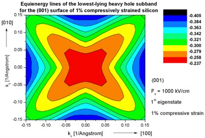 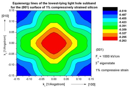
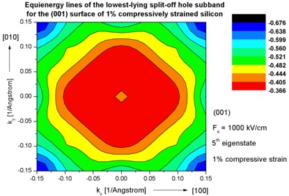
Note: The color map figures have a rectangular shape although they
should be quadratic.
Step 11: k|| dispersion of a strained silicon inversion layer
with (001)
surface orientation that is uniaxially compressed along the [110] direction
-> 1DSi_triangular_strained_uniaxial_comp_001surface_read_in.in

->
strain_cr1D_read_in_uniaxial110_1GPa.dat
(uniaxial strain file to be read in)
The following figures aim to reproduce Fig. 3 of the following paper:
E. Wang, P. Matagne, L. Shifren, B. Obradovic, R. Kotlyar,
S.Cea, J. He, Z. Ma, R. Nagisetty, S. Tyagi, M. Stettler, M.D. Giles
Quantum mechanical calculation of hole mobility in silicon
inversion layers under arbitrary stress
IEDM Technical Digest, San Francisco, USA, 147 (2004)
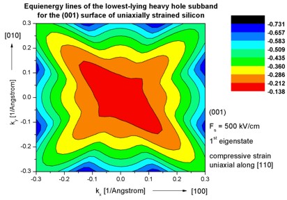 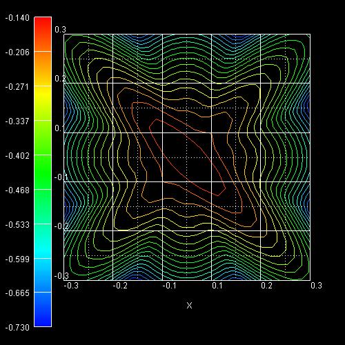
They show the equienergy lines of the lowest lying heavy hole subband
for the (001) surface of uniaxially, compressively strained
silicon calculated using a strain dependent 6-band k.p Hamitonian. Only one spin
state is plotted for clarity.
The x and y axes represent kx and ky in units of
[1/Angstrom]. The x axis points along the [100], the y axis along the [010]
direction of the crystal coordinate system.
The uniaxial strain is directed along the [110] direction. The applied stress is
1 GPa (compressive) and corresponds to the following nonzero strain tensor
components:
  exx = eyy = -0.00275

  ezz =  0.00215

  exy = -0.003125
The inversion layer is oriented in the (001) plane and has been modeled
assuming a triangular well potential corresponding to an electric field of Fs =
-500 kV/cm.
Clearly, the anisotropic nature of the energy surface drastically affects the
scattering rates and thus the hole mobility tensor.
How to make use of nextnanomat's Template feature to sweep over variable
values...
Open nextnanomat, Go to 'Template' tab, Open Template file.
- To vary between unstrained, compressive strain, and
tensile strain, do the following:
In 'Sweep' select 'List of values', Select variable
'SubstrateLatticeConstant', Click on 'Create input files'.
- To do the calculations for different electric fields:
In 'Sweep' select 'Range of values', Select variable
'ElectricFieldStrength', Click on 'Create input files'.
(Note: In order to be able to compare the eigenenergies of different
electric field simulations with each other, we adjust the variable
band-shift automatically.
Then all eigenenergies are with respect to a common reference energy. See
input file for more information.)
- You can do the same simulations for [001] and [011] growth
directions simultaneously.
In 'Sweep' select 'List of values', Select variable 'hkl_z_direction', Click
on 'Create input files'.
(Note: This does not work for [111]. You have to uncomment the relevant
lines in the input file instead.
Go to Run tab, Start simulations
You can do several simulations in parallel: Tools ==> Options
==> maximum number of simulatenously simulations.
|