|
| |
nextnano3 - Tutorial
next generation 3D nano device simulator
1D Tutorial
k.p dispersion in bulk, biaxially strained and uniaxially strained Si
Author:
Stefan Birner
If you want to obtain the input files that are used within this tutorial, please
check if you can find them in the installation directory.
If you cannot find them, please submit a
Support Ticket.
-> 1Dbulk_kp_dispersion_Si.in
-
(unstrained)
-> 1Dbulk_kp_dispersion_Si_3Dplot.in
-
-> 1Dbulk_kp_dispersion_strained_Si.in -
-> 1Dbulk_kp_dispersion_strained_Si_3Dplot.in -
-> 1Dbulk_kp_dispersion_uniaxial_strained_Si_read.in -
-> 1Dbulk_kp_dispersion_uniaxial_strained_Si_3Dplot_read.in -
strain_cr1D_read_in_uniaxial110.dat
Band structure of bulk Si
- We want to calculate the dispersion E(k) from |k|=0 nm
-1 to |k|=0.1
nm-1 along the
following directions in k space:
- [110] to [000] where [000] is the Gamma point.
- [000] to [100]
We compare 6-band k.p theory results vs. single-band (effective-mass)
results.
- We calculate E(k) for bulk Si (unstrained).
Bulk dispersion along [1100] and [100]
-> 1Dbulk_kp_dispersion_Si.in
  $output-kp-data

 destination-directory    = kp/


 bulk-kp-dispersion       = yes

   grid-position            = 2d0                      !
in units of [nm]
!----------------------------------------
! Dispersion along [110] direction
! Dispersion along [100] direction
! maximum |k| vector = 1.0 [1/nm]
!----------------------------------------
k-direction-from-k-point =
0.7071d0 0.7071d0
0d0 ! k-direction and range for dispersion plot [1/nm]
The maximum value of |k| is SQRT(0.7071² + 0.7071²) = 0.1 [1/nm].
k-direction-to-k-point = 1.0d0 0d0 0d0 !
 [1/nm]


 number-of-k-points       = 100                     !
number of k points to be calculated (resolution)
 shift-holes-to-zero      = yes
  ! 'yes'
or 'no'
$end_output-kp-data- We calculate the pure bulk dispersion at
grid-position = 2d0,
i.e. for the material located at the grid point at 2 nm. In our case this is
Si but it could be any strained alloy. In the latter case, the k.p
Bir-Pikus strain Hamiltonian will be diagonalized.
The grid point at grid-position must be located inside a quantum cluster.
shift-holes-to-zero = yes forces the
top of the valence band to be located at 0 eV.
How often the bulk k.p Hamiltonian should be solved can be specified
via number-of-k-points. To increase the resolution, just increase
this number.
- Start the calculation.
The results can be found in:
kp_bulk/bulk_6x6kp_dispersion_as_in_inputfile_kxkykz_000_kxkykz.dat
kp_bulk/bulk_sg_dispersion.dat (single-band approximation)
- Note that for values of |k| larger than 0.1, k.p theory might not
be a good
approximation any more.
Step 2: Plotting E(k)
- Here we will have to visualize the results of both Step 1 and Step 2.
- The final figure will look like this:
(In silicon, the directions [100], [010], [001], [-100], [0-10] and [00-1] are
equivalent in the unstrained case
and so are the directions [110], [101], [011], [-110], [-101], [0-11], [1-10],
[10-1], [01-1], [-1-10], [-10-1] and [0-1-1].)
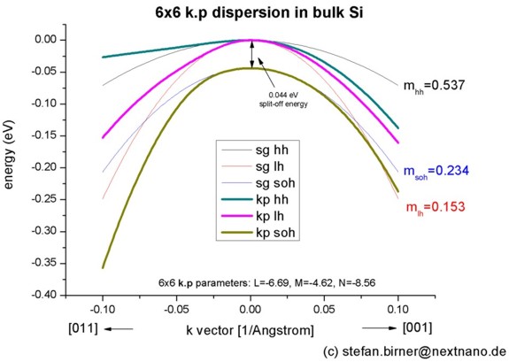
The split-off energy of 0.044 eV is identical to the split-off energy as
defined in the database:
6x6-kp-parameters = ... 0.044d0
In the unstrained case, the light hole seems to be kind of
isotropic in contrast to the heavy and split-off hole which clearly exhibit
anisotropy. The light hole "isotropy" can be checked further below in the 2D
and 3D plots of the dispersion curves.
For comparison, the single-band (effective-mass) dispersion is
also shown. It corresponds to the following effective hole masses:
 valence-band-masses = 0.537d0 0.537d0
  0.537d0 ! [m0]
heavy hole
0.153d0 0.153d0 0.153d0 ! [m0]
0.234d0 0.234d0 0.234d0 ! [m0]
The effective mass approximation is a simple parabolic dispersion which is
isotropic (i.e. no dependence on the k
vector direction).
One can
see that for |k| < 0.1 [1/nm] the single-band approximation is in good
agreement with 6-band k.p but
differ at larger |k| values substantially.
Plotting E(k) in three dimensions
-> 1Dbulk_kp_dispersion_Si_3Dplot.in
Alternatively one can print out the 3D data field of the bulk E(k) =
E(kx,ky,kz) dispersion.
  $output-kp-data
  ...
  bulk-kp-dispersion-3D =
  yes
  grid-position
  = 2d0              !
in units of [nm]
!----------------------------------------
! maximum |k| vector = 1.0 [1/nm]
! maximum |k| vector = 1.5 [1/nm]
!----------------------------------------
!
Note: The 3D and 1D plots in the tutorial use "1.0d0",
the 2D plots use "1.5d0".
  k-direction-to-k-point =
1.0d0 0d0 0d0 ! [1/nm]
! k-direction-to-k-point =
1.5d0 0d0 0d0 !
(2D plot) k-direction and range for dispersion plot [1/nm]
number-of-k-points = 40
!
number of k points to calculated (resolution)
  shift-holes-to-zero   =
  yes
! 'yes' 'no'
The meaning of number-of-k-points = 40
is the following:
40 k points from '- maximum |k| vector'
to zero (plus the Gamma point) and
40 k points from zero to '+ maximum |k| vector'
(plus the Gamma point)
along all three directions,
i.e. the whole 3D volume then contains 81 * 81 * 81 = 531441
k points.
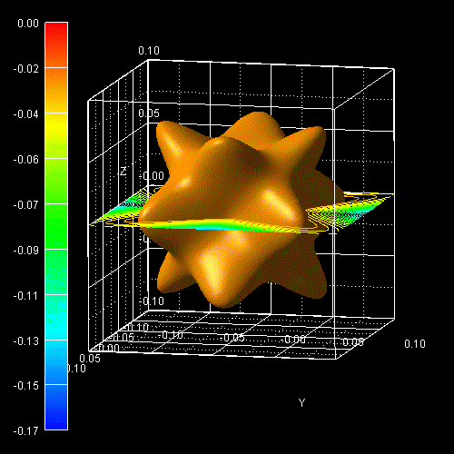
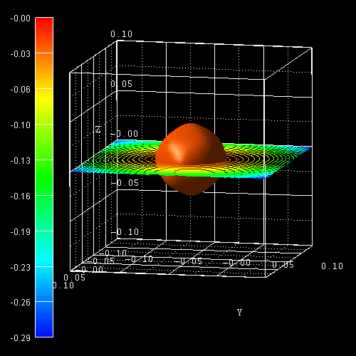
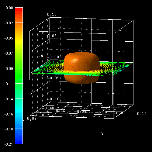
The following figure shows the constant energy surface at E = 25 meV below the
valence band edge for the heavy hole (left) and for the light hole
(right).
In the unstrained case, both heavy and light hole are degenerate at
k =
0. The color bars on the left side of each plot correspond to the 2D
slices in these pictures. The units are [eV].
The following figure shows the constant energy contours in the (kx,ky)
plane of a 2D slice through the heavy hole (left) and the light hole
(right) 3D E(kx,ky,kz)
dispersion at kz = 0, i.e. E(kx,ky,0). The
light hole is much more isotropic than the heavy hole.
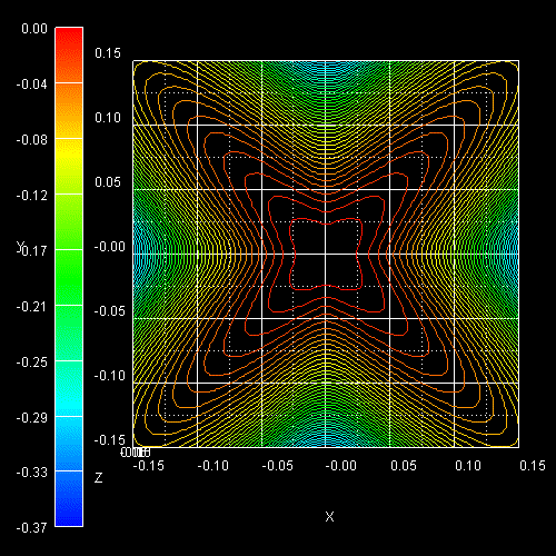 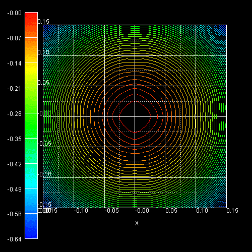
These two figures are in very good agreement with the figures in the following
paper:
Key Differences For Process-induced Uniaxial vs. Substrate-induced Biaxial
Stressed Si and Ge Channel MOSFETs
S.E. Thompson, G. Sun, K. Wu, J. Lim, T. Nishida
Proc. IEEE-IEDM (International Electron Devices Meeting), 221 (2004)
Note that the figures in the paper were calculated using the empirical
pseudopotentials method whereas ours are based on a 6-band k.p
Hamiltonian.
Technical details: For the 3D plots we calculated the E(k)
dispersion until a maximum k vector of kx = ky =
kz = 1.0 nm-1 (k-direction-to-k-point = 1.0d0 0d0 0d0)
whereas for the 2D plots we used a maximum k vector of kx =
ky = kz = 1.5 nm-1 (k-direction-to-k-point =
1.5d0 0d0 0d0) as was done in the figures
in the paper of S.E. Thompson et al. Thus the color bars at the left side of
the figures differ between 2D and 3D.
Band structure of strained Si
- Now we perform these calculations again for Si that is biaxially strained
with respect to Si0.83Ge0.17. The Si0.83Ge0.17 lattice
constant is larger than the Si one, thus Si is strained tensilely.
- The changes that we have to make in the input file are the following:
  $simulation-flow-control

 ...

 strain-calculation  = homogeneous-strain


  $end_simulation-flow-control
  $domain-coordinates

 ...

 pseudomorphic-on    = Si(1-x)Ge(x)

 alloy-concentration = 0.17d0


  $end_domain-coordinates
As substrate material we take (relaxed) Si0.83Ge0.17
and
assume that Si is strained pseudomorphically (homogeneous-strain)
with respect to this substrate, i.e. Si is subject to a biaxial tensile
strain.
-> 1Dbulk_kp_dispersion_strained_Si.in
The figure shows the E(k) dispersion along the [110] and [100]
(=[010]) directions
for biaxially, tensilely strained silicon. Note that the heavy and light holes
are now "mixed" and not any longer "purely" heavy and light hole states. At
the zone center (k = 0), the highest valence band has light hole
character.
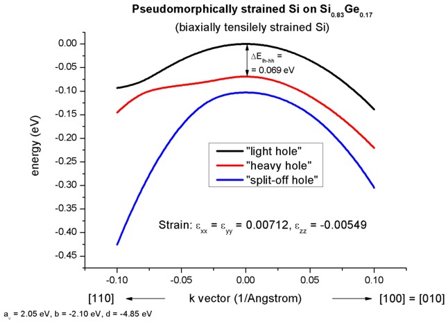
(In silicon, the directions [100], [010], [-100] and [0-10] are equivalent in
the biaxially strained case if the biaxial
stress is directed along the [100], [-100], [010] and [0-10] directions.
The directions [110], [-110], [1-10] and [-1-10] are also equivalent.)- Due to the positive hydrostatic strain (i.e. increase in volume or
negative hydrostatic pressure) we obtain a reduced band gap with respect to
the unstrained Si (not shown in the figure).
Furthermore, the degeneracy of the heavy and light hole at k=0 is
lifted by 69 meV and the light hole has been shifted above the heavy hole.
Now, the anisotropy of the holes along the different directions [100] and
[110] is very pronounced. There is even a band anti-crossing along [110].
This biaxial strain can be expressed as applied stress (sigmaij) in
units of GPa. The elastic constant of Si are:
  elastic-constants = 165.77d0 63.93d0
  79.62d0 ! c11,c12,c44 [GPa]
298
K [Landolt-Boernstein]
=>
=> sigmaxx = sigmayy = (c11 + c12
) * e||
+ c12 * e|| = 1.2845 GPa
(e|| = exx = eyy ;
e_|_
= ezz)
- Note that in the strained case, the effective-mass approximation is very poor.
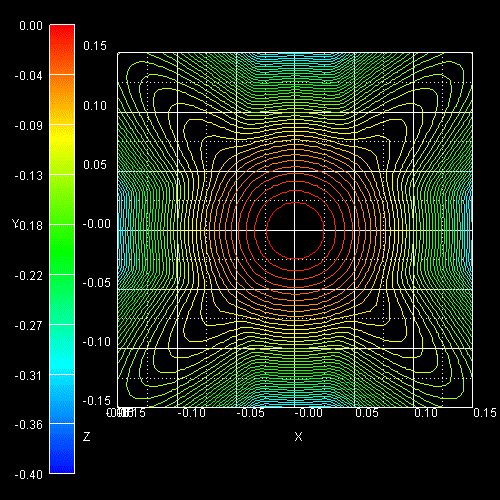
-> 1Dbulk_kp_dispersion_strained_Si_3Dplot.in
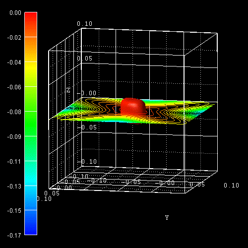
The following figure shows the constant energy contours in the (kx,ky)
plane of a 2D slice through the ground state hole (left) and the
first excited hole state
(right) 3D E(kx,ky,kz)
dispersion at kz = 0, i.e. E(kx,ky,0).
At the left figure one can see that around k = 0, the highest
hole state has "light" hole character and for larger k values the
"heavy" hole character dominates.
At the right figure, the second highest hole state is shown which is separated
by 0.069 eV from the "light" hole (valence band edge). Around k = 0
it has heavy hole character and at larger k values it has "light" hole
character as can be understood by comparing these plots to the unstrained
dispersion curves.
 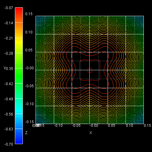
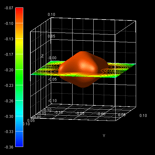
The following figure shows the constant energy surface at E = 25 meV below the
valence band edge for the ground state hole (left) and the constant
energy surface at 94 meV below the valence band edge for the first excited hole
state
(right) (69 meV + 25 meV = 94 meV).
The degeneracy of heavy and light hole at
k =
0 is lifted by 69 meV. The color bars on the left side of each plot correspond to the 2D
slices in these pictures. The units are [eV].
Reading in arbitrary strain tensors
Sometimes the user might want to specify an arbitrary strain tensor as input,
read it in and calculate the relevant E(k) dispersion.
The procedure to do this is the following:
	$simulation-flow-control

 ...

 strain-calculation = import-strain-crystal-coordinate-system
  $import-data-on-material-grid

 source-directory = strain/

 filename-strain  = strain_cr1D_read_in_uniaxial110.dat


  $end_import-data-on-material-grid
The file strain/strain_cr1D_read_in_uniaxial110.dat
must contain the strain tensor in the following format:
   coordinate   exx  eyy
  ezz  exy  exz  eyz
The units for coordinate are [nm]. The strain tensor
units are dimensionless [-].
The strain tensor refers to the crystal coordinate system in this example.
Note: The eij components refer to shear strain
and not to "engineer shear strain".
Shear strain is the average of two strain tensor components, i.e.
eij = 1/2 (dui/dxj + duj/dxi)
whereas engineer shear strain is defined as the total shear strain
eij = dui/dxj + duj/dxi.
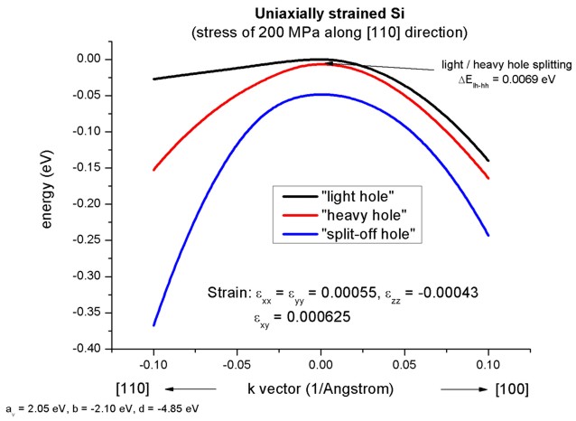
Example: Reading in uniaxial strain...
We read in the following strain tensor which corresponds to a small uniaxial
tensile strain along the [110] direction (corresponding to a [110] stress of
sigma = 200 MPa):
  exx = eyy = 0.00055

  ezz = -0.00043

  exy =  0.000625
It can be calculated by using these formulas where Sij
is the contracted notation of the forth-rank compliance tensor Sijkl:
 exx = eyy = (S11 + S12) *
sigma / 2 = (7.681 + (-2.138)) [1/TPa] * 200 [MPa] / 2 = 0.00055

 ezz = S12 * sigma = -2.138 [1/TPa] * 200 [MPa] =
-0.00043

 exy = S44 * sigma / 2
 = 12.56 [1/TPa] * 200 [MPa] /
2 = 0.001256
To convert the "engineer shear strain definition" into the strain tensor
definition used within nextnano³, one has to divide exy
by a factor of 2 and thus one obtains exy =
0.000628, i.e. the equation to be used reads:
 exy = S44 * sigma / 4
= 12.56 [1/TPa] * 200 [MPa] / 4 = 0.000628
This only applies to the offidagonal components eij
of the strain tensor.
cij
can be converted into Sij
by using the following formulas (P. Y. Yu, M. Cardona, "Fundamentals of
Semiconductors, 3rd ed., p.140)
  c44 = 1/S44     => S44
= 1/c44 = 1/79.62 [GPa] = 12.56
[1/TPa]
= 12.70(9) [1/TPa]
  c11 -  c12 = 1 / (S11 -  S12)
= 165.77 -
63.93 = 101.84 [GPa]

  c11 + 2c12 = 1 / (S11 + 2S12)
= 165.77 + 2 * 63.93
= 293.63 [GPa]


  => S11 =  7.681   [1/TPa]
= 7.73(8) [1/TPa]
=> S12 = -2.138 [1/TPa]
= −2.15(4) [1/TPa]
The color bars on the left side of each plot correspond to the 2D
slices in these pictures. The units are [eV].
-> 1Dbulk_kp_dispersion_uniaxial_strained_Si_3Dplot_read.in
 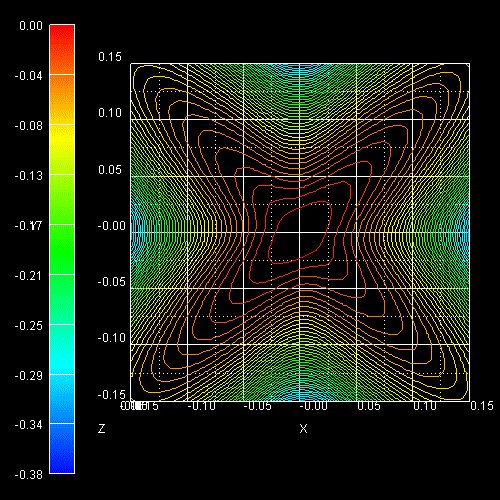
This figure shows the E(k) dispersion along the lines from zero to [100]
and from [110] to zero. Note that the directions [110] and [-110] are no
longer equivalent as can be seen in the 2D plot shown above.
-> 1Dbulk_kp_dispersion_uniaxial_strained_Si_read.in
|